
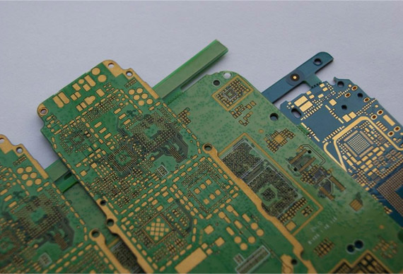


HDI PCB / BLIND&BURIED VIA HOLE PCB / BVH PCB
SPEEDAPCB has been focusing on the production of various PTH (plated through hole PCB), buried via hole PCB and blind via hole PCB, and HDI PCB prototype.
When it comes to blind and buried hole circuit boards, everyone thinks of HDI boards. Generally, there are more blind and buried hole circuit boards used in mobile phones or navigation instruments. Such PCB boards require high technical content and accurate accuracy. Of course, the price is compared with other It is also high for multilayer circuit boards.
HDI high density interconnect pcb : 1 + n + 1, 1 + 1 + n + 1 + 1, 2 + n + 2, 3 + n + 3,
Features of Blind&Buried Via Hole PCB
HDI PCB
Blind Via Hole is the connection between the outermost circuit in the PCB and the adjacent inner layer with a plated hole. Because the opposite side cannot be seen, it is called blind pass. In order to increase the space utilization between the circuit layers of the board, blind holes come in handy. The blind hole is a via hole to the surface of the printed board.
Buried Via Hole, the connection between any circuit layers in the PCB, but there is no conduction with the outer layer, that is, there is no meaning of a via hole extending to the surface of the circuit board.
HDI PCB
The blind holes are located on the top and bottom surfaces of the circuit board and have a certain depth. They are used to connect the surface layer circuits to the inner layer circuits below. The depth of the holes generally has a prescribed ratio (aperture). This manufacturing method requires special attention, and the drilling depth must be just right. Failure to pay attention will cause difficulties in plating inside the hole. Therefore, few factories will adopt this production method. In fact, it is possible to drill the holes of the circuit layers that need to be connected beforehand, and then glue them together, but they need more precise positioning and alignment devices.
HDI PCB
This manufacturing process cannot be achieved by bonding the circuit boards and then drilling. It is necessary to perform the drilling operation at the individual circuit layer, firstly locally bond the inner layer, then perform plating treatment, and finally all the bonding. Because the operation process is more laborious than the original vias and blind holes, the price is also the most expensive. This manufacturing process is usually only used for high-density circuit boards, increasing the space utilization of other circuit layers.
HDI PCB
In the PCB manufacturing process, drilling is very important. The simple understanding of drilling is to drill the required via holes on the copper clad board, which has the function of providing electrical connections and fixing devices. If the operation of the via is caused by incorrect operation, the device cannot be fixed on the circuit board, which will affect the use of the circuit board, and the entire board will be scrapped. Therefore, the process of drilling is very important.
Parameters of Blind&Buried Via Hole PCB
|
Items |
Capability. |
|
|
Max board size |
580X700mm |
|
|
Boar Material |
FR-4,Aluminum, High Tg FR4,CEM3,etc. |
|
|
Min trace width/ space (inner layer) |
4mil/4mil(0.1mm/0.1mm) |
|
|
Min PAD (inner layer) |
5 mil(0.13mm) |
|
|
Min thickness(inner layer) |
4 mil(0.1mm) |
|
|
Inner copper thickness |
0.5~4 oz |
|
|
Outer copper thickness |
0.4~6 oz |
|
|
Finished board thickness |
0.4-3.2 mm |
|
|
Board thickness tolerance control |
±0.10 mm |
±0.10 mm |
|
±10% |
±10% |
|
|
±10% |
±10% |
|
|
Inner layer treatment |
brown oxidation |
|
|
Layer count Capability |
1-30 LAYER |
|
|
alignment between ML |
±2mil |
|
|
Drill hole diameter |
0.15mm-0.65mm |
|
|
Aspect ratio of plated hole |
10: 01 |
|
|
Hole precision |
±2 mil(±0.05mm) |
|
|
tolerance for Slot |
±3 mil(±0.75mm) |
|
|
Hole diameter tolerance(PTH) |
±3 mil(±0.075mm) |
|
|
Hole diameter tolerance(NPTH) |
±1mil(±0.025mm) |
|
|
Max Aspect Ratio for PTH |
8: 01 |
|
|
Hole wall copper thickness |
15-50um |
|
|
Alignment of outer layers |
4mil/4mil |
|
|
Min trace width/space for outer layer |
4mil/4mil |
|
|
Tolerance of Etching |
+/-10% |
|
|
Thickness of solder mask |
on trace |
|
|
Thickness of solder mask |
at trace corner |
≥0.2mil(5um) |
|
Hardness of solder mask |
On base material |
≤+1.2mil |
|
6H |
Finished thickness |
|
|
Alignment of solder mask film |
±2mil(+/-50um) |
|
|
Min width of solder mask bridge |
4mil(100um) |
|
|
Max hole with solder plug |
0.5mm |
|
|
Surface treatment |
HAL (Lead or Lead free), immersion Gold, Immersion Nickel, Electric Gold finger, plated Gold, OSP, Immersion Silver.carbon oil,etc. |
|
|
Max Nickel thickness for Gold finger |
280u"(7um) |
|
|
Max gold thickness for Gold finger |
30u"(0.75um) |
|
|
Nickel thickness in Immersion Gold |
120u"/240u"(3um/6um) |
|
|
Gold thickness in Immersion Gold |
2u"/6u"(0.05um/0.15um) |
|
|
Impedance control and its tolerance |
50±10%,75±10%,100±10% 110±10% |
|
|
Trace Anti-stripped strength |
≥61B/in(≥107g/mm) |
|
|
bow and twist |
0.75% |
|
We provide printed circuit board supplies,hdi pcb board,hdi printed circuit boards,hdi pcb prototype,hdi circuit boards,high density interconnect pcb,high density pcb,buried via pcb and buried vias pcb,RFQ today.
Personne à contacter : Molly Tu speedapcb, +86 0731 15387574935
Bonne affaire : acheter au vendeur
Nous vous invitons à lire nos conditions générales d'utilisations. Vous pouvez aussi vous rendre sur nos FAQ et consulter notre page d'informations sur les risques liés à la contrefaçon.
|
Cette page concerne les importateurs et exportateurs de HDI PCB / BLIND&BURIED VIA HOLE PCB / BVH PCB Rechercher dans la catégorie : Divers Rechercher dans la catégorie : hole, blind&buried |
Signalez un abus
Tuesday 26 May 2026
Quantité : 108
Product Details Bed Type : Panel Layer : 2 layers Frame Material : Metal Color : Pink, Blue, Cream white, Browm… Headboard Included: Yes Under bed Storage : No Product Care : Wipe with a clean, damp cloth Painted frame · One set include - Headboard. - Footboard. - Two...
Qui Phuc Company Limited
- Luck06
- 700000 - Ho Chi Minh
- +84 9 86 58 28 62
Signalez un abus
Saturday 23 August 2014
LED RVB Meubles avec 16 couleurs par télécommande et batterie rechargeable Li-batterie Accessories Manuel d'utilisation, télécommande IR, Chargeur Télécommande Télécommande IR (5m) Télécommande sans fil (20-60m) Chargeur fiche Euro Type, BS fiche, prise américaine, AU...
Signalez un abus
Tuesday 24 November 2015
Quantité : more than
Application The cables are similar in design and application to CW 1308, but with Low Smoke Halogen Free cores and sheath. CW 1600 has the added advantage of an Aluminium/Polyester foil screen and drain wire. A fire barrier tape is included on cable with more than 6 pairs. The cables...
caledonian cables limited
- 999077 - hongkong
- +85 2 21 16 10 40
- 852 21161040
Paiement sécurisé